Graduate student Yucheng Yang with Professor Matt Rosenberger and collaborators at Columbia University, New York, and the National Institute for Materials Science, Tsukuba, Japan, have demonstrated a new method to characterize intrinsic defects in atomically-thin semiconductors based on lateral force microscopy (LFM). Their paper is accepted for publication by the American Chemical Society in ACS Nano. LFM extracts information with atomic spatial resolution from signals generated by the interaction of a laterally translated nanoprobe over a material surface. The published results are achieved in a commercial atomic force microscope under common ambient lab conditions. The method is applicable across conducting and insulating materials and enables routine defect−property determination and needed materials understanding. Yucheng is a doctoral student in the Notre Dame interdisciplinary Materials Science & Engineering program in the Aerospace and Mechanical Engineering Department. Two-dimensional materials are receiving increased attention for ultimately-scaled transistors as well as for wide-ranging device and sensor applications where understanding and control of defects is key.
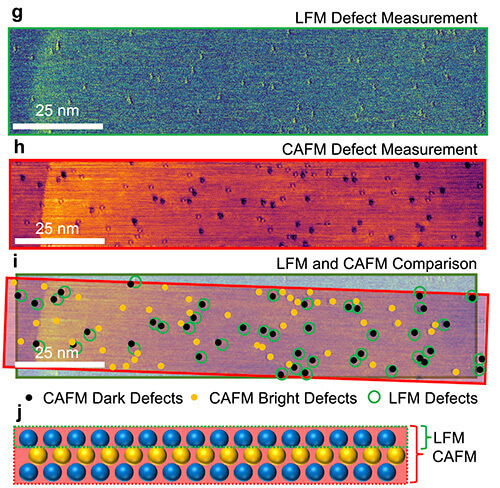
Figure. (g) Lateral force microscope (LFM) image, (h) Conductive atomic force microscope (CAFM) image, (i) overlay of LFM and CAFM defect locations. Black dots correspond to high conductivity (“dark”) defects and yellow dots correspond to low conductivity (“bright”) defects in CAFM. Green circles correspond to defects in LFM. (j) A schematic showing the difference between LFM and CAFM defect measurement techniques in the number of atomic layers each technique can measure. CAFM measures defects in more atomic layers than shown here, but LFM measures the top atomic layer.